Nanometrics
Nanometrics
Request for consultation
As an authorized sales representative of Nanometrics, Inc., Toho Technology provides Material Characterization systems to customers in all states east of the Mississippi River, Texas, New Mexico, and Canada.
Photoluminescence (PL) Mapping
III-V semiconductors get excited by a laser at a wavelength above their band gap. The photon energy applied to the material will force carriers into the conductance band. Once the excitation ends, the carriers will recombine in the valence band and emit photon energy. The characteristics of these emitted photons is a signature of the material characteristics and gives information about the composition and structure of the material.
The PL signature of a material can tell you about the material properties and – if a full wafer is mapped – give critical information about reactor health, final device performance and give an early indication about the final device performance.

Parameters to be controlled using photoluminescence are:
Peak Wavelength — Eg / Composition
FWHM — Composition Variation
Peak & Integrated Intensity — Defects / Crystal Quality / Impurities (O2)
Maps — Uniformity & Electrically Active Material / Surface Defects
Nanometrics PL metrology lineup provides very flexible metrology solutions for different use cases:
RPMBlue: LED reactor monitoring
RPMBlue-FS: Multi-purpose PL mapper for UV, VIS and IR applications
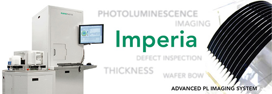
Imperia: PL/thickness and defect inspection system for production control
Vertex: Multi-purpose R&D and production monitoring
Products

Imperia

RPM Blue

RPM Blue-FS

Vertex
As an authorized sales representative of Nanometrics, Inc., Toho Technology provides Material Characterization systems to customers in all states east of the Mississippi River, Texas, New Mexico, and Canada.
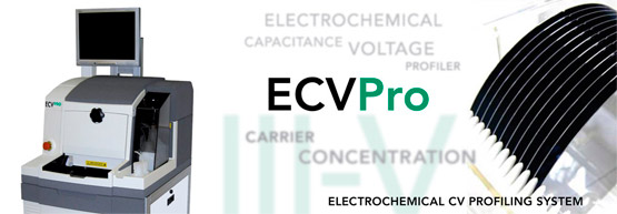
CV Profiling
Measuring the carrier concentration in materials can be done several ways. Hall Effect metrology is a very efficient way to measure the carrier concentration in bulk materials. If there is a need to measure carrier concentration as a function of depth, there is destructive methods available only. Nanometrics’ patented approach to carrier concentration profiling includes high resolution faradaic etching, forming a schottky diode and measure the C-V curve. This method is very efficient and provides a good alternative to expensive analysis methods such as SIMS. While etching through p-type materials is rather easy, light is required to etch though n-type materials. The ECVpro offers a visible light source for the majority of III-V semiconductors. Once you need to etch through wide band gap materials such as GaN, an optional UV-light source is available as well. Special etch algorithm also ensure smooth etching through highly defective materials or materials with high metallic content.

Products
ECV Pro
As an authorized sales representative of Nanometrics, Inc., Toho Technology provides Material Characterization systems to customers in all states east of the Mississippi River, Texas, New Mexico, and Canada.
Fourier Transform Infrared Metrology
The goal of any absorption spectroscopy is to measure how well a sample absorbs light at each wavelength. The most straightforward way to do this, the “dispersive spectroscopy” technique e.g. reflectometry.
Fourier transform spectroscopy is a less intuitive way to obtain the same information. This technique shines a beam containing multi-wavelength infrared light, and measures how much of that beam is absorbed by the sample. This method is very well suited to measure thick epitaxial materials which have a high absorbance in the visible wavelength range such as Si. By adding a transmission detector underneath the wafer surface, the transmitted spectrum of infrared light travelling through the material can be analyzed for presence of contaminating materials such as carbon, oxygen or hydrogen in Si substrates.
There are many applications which benefit from the FTIR technique:
Substrate thickness
Thickness of epitaxial materials
SiC epi layer & substrate thickness
B and P concentration in PSG, BSG and BPSG
CO – Substitutional carbon and interstitial oxygen in silicon substrates
SolarSiCO – Substitutional carbon and interstitial oxygen in thin silicon substrates
FSG – Fluorine content of FSG
SiN – Measures hydrogen in silicon nitride films
HSQ – Hydroxyl and hydrogen content in oxides SOG, FOX
SiON – Oxygen, nitrogen and hydrogen in SiON.
SiCN – Carbon in SiCN
SiOC – Carbon in SiOC
Oxygendose – Measurement of oxygen implant dose at SIMOX process
Oxygen Precipitate – Measurement of oxygen precipitates in Si substrates
Products

QS 1200

QS 2200

QS 3300

Stratus
As an authorized sales representative of Nanometrics, Inc., Toho Technology provides Material Characterization systems to customers in all states east of the Mississippi River, Texas, New Mexico, and Canada.
Hall Effect Measurement
Named after its inventor, Edwin Hall, in 1879, Hall Effect metrology is a very fast and effective way obtaining material characteristics for research and development. The Hall effect is basically the production of a voltage difference (the Hall voltage) across an electrical conductor, transverse to an electric current in the conductor and a magnetic field perpendicular to the current.

The Hall coefficient is defined as the ratio of the induced electric field to the product of the current density and the applied magnetic field. It is a characteristic of the material from which the conductor is made, since its value depends on the type, number, and properties of the charge carriers that constitute the current. Using Hall Effect measurement, the following properties can be determined:
Resistivity/Conductivity
Mobility
Bulk/Sheet carrier concentration
Doping type
Hall coefficient
Magnetoresistance
Vertical/Horizontal ratio of resistance
Shubnikow-de Haas Oscillations (SdH)
Products

HL5500
As an authorized sales representative of Nanometrics, Inc., Toho Technology provides Material Characterization systems to customers in all states east of the Mississippi River, Texas, New Mexico, and Canada.
Film Analysis
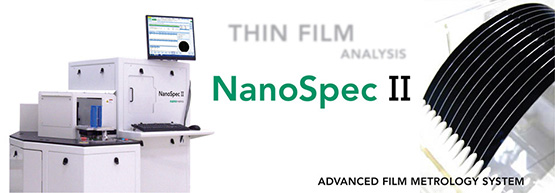
Using reflectometry to obtain parameters such as thickness, absorption coefficient and refractive index is a very mature technique. Nanometrics expertise in this field dates back into the early 1970’s. For years, the Nanospec metrology series has been the reference in optical metrology using reflectometry.
Every transparent material is characterized by its dispersion curve. The dispersion defines, how much light is absorbed by the material and how much light is refracted. These two parameters vary over wavelength and are specific to every material. When light travels through a material and is reflected by a substrate, it will form a interference pattern with the surface reflected light. This interference pattern contains the parameters of the material such as thickness (T), refractive index (n) and absorption coefficient (k).

To extract these parameters from the reflected light, a model is laid over the experimental light spectrum and the model parameters are floated until the model matches the experimental light spectrum.
While the optical setup of a reflectometer does have a significant influence to the quality of data and accuracy of a measurement, the modeling capabilities contribute as well. Nanometrics newest generation of table top and standalone reflectometers benefit from more than 30 years of optical competence and our latest generation of analysis & modelling software – the industry leading NanoDiffract™ software. Even complicated multi-layer structures can be measured and modelled in an easy and intuitive way.
Products
Seeing
- ECV Pro
- HL Series (Hall Effect)
- Imperia
- NanoSpec II
- QS 1200
- QS 2200
- QS 3300
- RPMBlue
- RPMBlue-FS
- Vertex