
The tapes for semiconductor
THE TAPES FOR SEMICONDUCTOR
Application sector
Tape structure

Tape Performance

Test method: JIS Z 0237:2000
- Adhesion: Measured at 20 min after applying and pressing tape to each adherent using a 2 kg roller rolled back and forth once. 90º peel, pulling speed: 300 mm/min
- UV irradiation: High pressure mercury vapor lamp used. Irradiation was approximately 300 mJ/cm2.
(Intensity: approximately 75 mW/cm2 x approximately 4 seconds at 365 nm) - MD: Machine direction TD: transverse direction
Directions for use
(1) When this tape is not in use do not leave it exposed to light as this degrades the adhesive properties of this product. Place this tape in a light-shielding bag and take care not to be exposed to light as much as possible. It should not be exposed to sunlight and fluorescent lamps that contain strong UV light components degrading the adhesive properties of this product in a short period of time.
(2) Defective peeling and adhesive deposits tend to occur at excessively high UV intensities, high irradiation doses, and at high temperatures. Regarding UV irradiation, avoid using this tape at intensity higher than 100 mW/cm2 or irradiation doses exceeding 1000 mJ/cm2.
(3) Bonding or pickup may become impossible depending on the adherend materials, surface conditions, and the presence or absence of moisture or oil, etc. Consult us if you intend to use special applications and adherends.
(4) Store this tape in a cool dark location and use by the expiry date.
(5) Avoid direct hand contact with the adhesive surface.
(6) When this tape is applied to incorrect locations and needs to be reworked, please use a new tape.
(7) The figures shown in this TDS were obtained through in-house tests we believe to be reliable, but the accuracy of these values is not guaranteed.
(8) All the contents shown in this TDS are subject to change without notice.
(9) We assume no responsibility for any accidents caused by using this product. Carry out all evaluations before deciding to use this product.
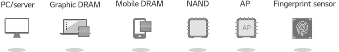
Application sector
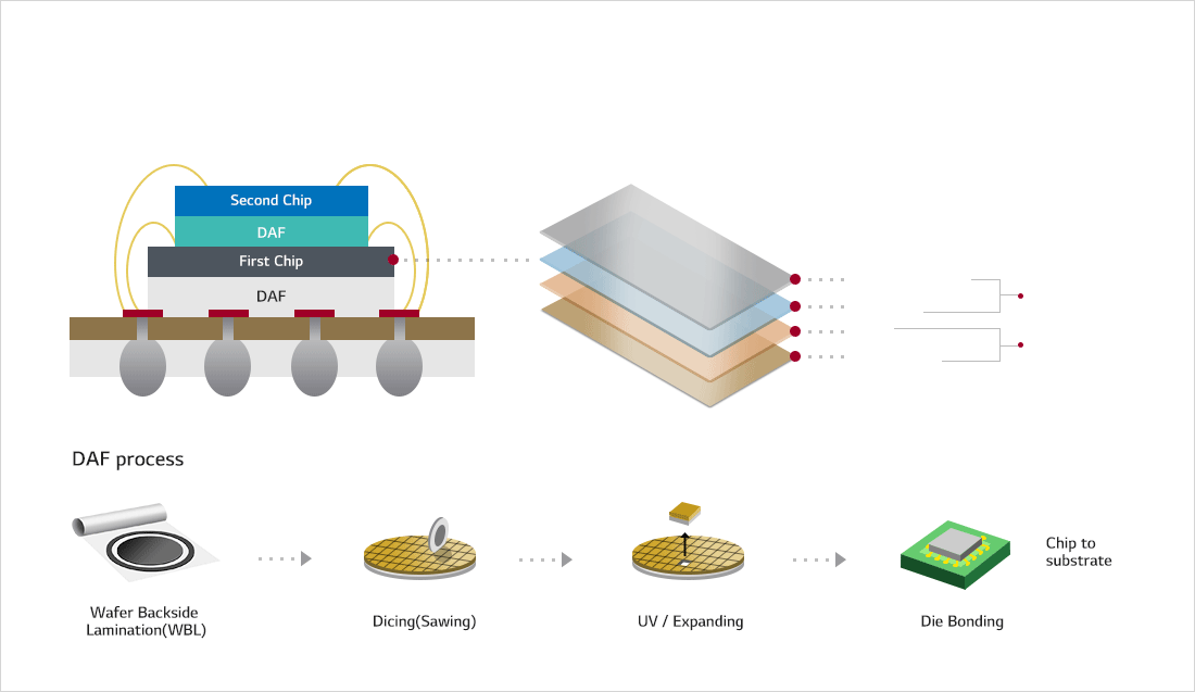
DAF(Die Attach Film) is an ultra-thin film adhesive used to connect semiconductor chips to circuit boards or chips to chips in the semiconductor packaging process. It is an essential material used in manufacturing flash memories, etc. in the post-manufacturing process of semiconductors. Lamination and manufacturing of thin layers of semiconductors are possible with its excellent reliability and easy processability.
Use of Product
Product functions and structure
Product classification
| Category | Thickness(μm)) | Features |
| General use (normal) | 5 / 10 / 20 |
|
| FOW (Film over Wire) | 50 ~ 80 |
|
| FOD (Film over Die) | 90 ~ 120 |
|
Application sector
Application sector
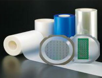
- + DICING TAPE
-
Application sector
- + UV Dicing Tape
-
Tape structure
Tape Performance
Test method: JIS Z 0237:2000
- Adhesion: Measured at 20 min after applying and pressing tape to each adherent using a 2 kg roller rolled back and forth once. 90º peel, pulling speed: 300 mm/min
- UV irradiation: High pressure mercury vapor lamp used. Irradiation was approximately 300 mJ/cm2.
(Intensity: approximately 75 mW/cm2 x approximately 4 seconds at 365 nm) - MD: Machine direction TD: transverse direction
Directions for use
(1) When this tape is not in use do not leave it exposed to light as this degrades the adhesive properties of this product. Place this tape in a light-shielding bag and take care not to be exposed to light as much as possible. It should not be exposed to sunlight and fluorescent lamps that contain strong UV light components degrading the adhesive properties of this product in a short period of time.
(2) Defective peeling and adhesive deposits tend to occur at excessively high UV intensities, high irradiation doses, and at high temperatures. Regarding UV irradiation, avoid using this tape at intensity higher than 100 mW/cm2 or irradiation doses exceeding 1000 mJ/cm2.
(3) Bonding or pickup may become impossible depending on the adherend materials, surface conditions, and the presence or absence of moisture or oil, etc. Consult us if you intend to use special applications and adherends.
(4) Store this tape in a cool dark location and use by the expiry date.
(5) Avoid direct hand contact with the adhesive surface.
(6) When this tape is applied to incorrect locations and needs to be reworked, please use a new tape.
(7) The figures shown in this TDS were obtained through in-house tests we believe to be reliable, but the accuracy of these values is not guaranteed.
(8) All the contents shown in this TDS are subject to change without notice.
(9) We assume no responsibility for any accidents caused by using this product. Carry out all evaluations before deciding to use this product.
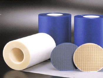
- + BG TAPE
-
Application sector
- + DAF
-
DAF(Die Attach Film) is an ultra-thin film adhesive used to connect semiconductor chips to circuit boards or chips to chips in the semiconductor packaging process. It is an essential material used in manufacturing flash memories, etc. in the post-manufacturing process of semiconductors. Lamination and manufacturing of thin layers of semiconductors are possible with its excellent reliability and easy processability.
Use of Product
Product functions and structure
Product classification
Category Thickness(μm)) Features General use (normal) 5 / 10 / 20 - Chip-to-chip or chip-to-board adhesive film
- Mold Void Free
- Can support various dicing processes such as Blade/GAL/DBG
FOW (Film over Wire) 50 ~ 80 - Wire-burial type adhesive film
- Pre-cure Void Free
- Has excellent fillet and wire burying ability
- Has excellent HAST reliability
FOD (Film over Die) 90 ~ 120 - Controller chip burial type adhesive film
- Pre-cure Void Free
- Has excellent controller chip and great void characteristic around wire
- Has excellent HAST reliability
- Can support various dicing processes such as Blade/GAL/DBG
- GAL process is possible
- + DICING TAPE HIGH TEMPERATURE - RESISTANT TAPE
-
Application sector
- + RELEASE FILM
-
Application sector